1D AlGaAs/GaAs Heterostructure
1. Abstract
This application note presents the simulation framework employed to analyse the energy band diagram and the formation of a two-dimensional electron gas (2DEG) in a one-dimensional (1D) AlGaAs/GaAs heterostructure.
2. Introduction
AlGaAs/GaAs heterostructures have been extensively studied [1-2], demonstrating that tailoring the band structure through precise control of material composition can result in the formation of a high-mobility conduction channel at the heterointerface.
The conduction band offset between AlGaAs and GaAs facilitates the transfer of electrons from the n-type AlGaAs donor layer into the lightly doped or un-doped GaAs region, where they accumulate at the interface. This accumulation forms a two-dimensional electron gas (2DEG), which exhibits both high carrier concentration and high mobility. Consequently, such structures are well suited for High Electron Mobility Transistors (HEMTs), widely employed in high-frequency applications [1].
The formation and characteristics of the 2DEG are strongly influenced by several parameters, including the aluminium mole fraction, doping concentration, and Schottky gate work function. These factors govern the conduction band profile and the degree of band bending at the heterointerface. In this application note, a one-dimensional AlGaAs/GaAs heterostructure is analysed using Aquarius TCAD simulations to investigate the conduction band profile, the formation of the 2DEG, and the impact of critical design parameters on device electrostatics.
3. Device Structure
3.1. Geometry
A schematic of the simulated AlGaAs/GaAs structure is shown in Fig. 1 with its key parameters summarised in Table 1.
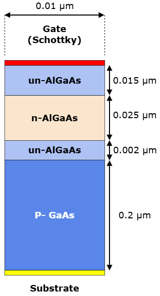
Fig. 1. 1D structure cell schematic.
Table 1: 1D structure layer doping concentration
| Layer | Doping Concentration |
|---|---|
| un-AlGaAs | 1E+13 cm-3 (Acceptor) |
| n-AlGaAs | 2E+18 cm-3 (Donor) |
| P- GaAs | 1E+14 cm-3 (Acceptor) |
3.2. Layer Mole Fractions
To investigate the effect of different compositions, the aluminium mole fraction (x) in the AlxGa1−xAs (n-AlGaAs) layer was varied from 0.2 to 0.4. This is done within the device editor by adjusting the mole fraction parameter in the region properties (see Fig. 2).
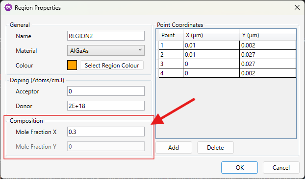
Fig. 2. Mole Fraction selection option in the region properties (example for n-AlGaAs layer).
This option is only available for ternary materials.
3.3. Mesh
Two different meshing approaches were implemented to discretise the 1D heterostructure: a structured mesh and an unstructured mesh.
The structured mesh provides a regular discretisation aligned with the layer stack, enabling targeted refinement along a single spatial direction (normal to the heterointerface). This is particularly advantageous for heterostructures, where the most significant variations occur vertically. As a result, higher resolution can be achieved in the critical region of band bending with fewer mesh elements, leading to improved numerical accuracy and reduced computational cost.
In contrast, the unstructured mesh offers greater geometric flexibility and can be easier to generate for more complex device layouts, though it may require a higher number of elements to achieve comparable resolution at the heterointerface.
The meshed device structures corresponding to the structured and unstructured approaches are presented in Fig. 3(a) and Fig. 3(b), respectively.

Fig. 3(a). Structured mesh.

Fig. 3(b). Unstructured mesh.
For the structured (grid-based) mesh, the refinement parameters are summarised in Table 2. A detailed comparison of the impact of these two meshing strategies on the simulation results, particularly in resolving the conduction band profile and 2DEG formation, is shown in the Simulation Results section.
Table 2: Mesh Refinement Settings
| Setting | Value |
|---|---|
| Number of Iterations | 2 |
| Refinement Variable | Distance from Junction |
| Distance | 0.4 μm |
| Reduction Factor | 0.5 |
In the unstructured mesh, the additional mesh box (hint size of 0.0005 µm) is introduced to accurately resolve the energy band-bending in the 2DEG region i.e. AlGaAs/GaAs interface (see Fig. 4).
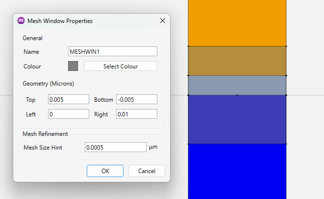
Fig. 4. The additional mesh box in the unstructured mesh structure.
The modified ‘Metallurgical Junction Refinement’ parameters in the mesh properties are shown in Table 3.
Table 3: Metallurgical Junction Refinement
| Setting | Value |
|---|---|
| Distance to Junction | 0.3 μm |
| Minimum Edge Length (Hint) | 0.001 μm |
| Maximum Edge Length (Hint) | 0.01 μm |
4. Simulation Setup
GaAs was used as the reference material throughout this study. Additionally, the effect of DX centers in the AlGaAs layer, which act as electron trapping centers and reduce the effective donor ionisation [3] was modelled using the incomplete ionisation model. The incomplete ionisation parameters are described in Table 4.
Table 4: Incomplete Ionisation parameters
| Parameter | Value | Units |
|---|---|---|
INCOMP_EA | 0 | eV |
INCOMP_ED | 0.06 | eV |
INCOMP_GA | 0 | - |
INCOMP_GD | 2 | - |
The simulation circuit used to generate the results is illustrated in Fig. 5. In this configuration, both the gate and substrate contacts are connected to ground, with no bias sweep applied during the operating point analysis (S1). This setup enables the evaluation of the equilibrium band structure of the device.
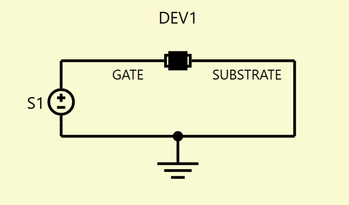
Fig. 5cmd. Simulated circuit.
For these simulations, the Schottky Gate bias and work function were set to 0 V and 5.2 eV, respectively.
5. Simulation Results
5.1. Formation of the 2DEG Channel
The conduction band energy and Fermi level were extracted along the vertical cutline C1, as shown in Fig. 6(b), using the simulation setup described above in Fig. 5.
A comparison of the conduction band-edge profiles obtained using structured and unstructured meshes is presented in Fig. 6(a) for the Al0.3Ga0.7As (X = 0.3)/GaAs heterostructure.
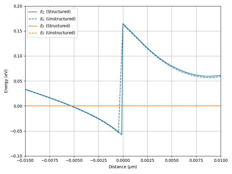
Fig. 6(a). Comparison of the conduction band and fermi level for structured and unstructured meshing.
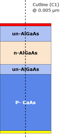
Fig. 6(b). Cutline location.
As shown in Fig. 6(a), the conduction band-edge at the AlGaAs/GaAs interface lies below the Fermi level, indicating the formation of a 2DEG channel. Both meshing approaches capture this behaviour. For this 1D heterostructure, the structured mesh provides improved resolution of the conduction-band profile at the heterointerface for a comparable mesh density. Since the dominant variation in the solution occurs in the y-direction, the structured mesh can concentrate elements normal to the interface, enabling finer discretisation in the region of strongest band bending. Consequently, the structured mesh was used for all subsequent simulations presented in this application note.
Using the circuit shown in Fig. 5, the gate voltage was swept between 0 V and -5 V. The recorded conduction band energy with fermi level and the electron concentration at 0 V, -0.5 V and -1.5 V are shown in Fig. 7 (a), (b) and (c), respectively.
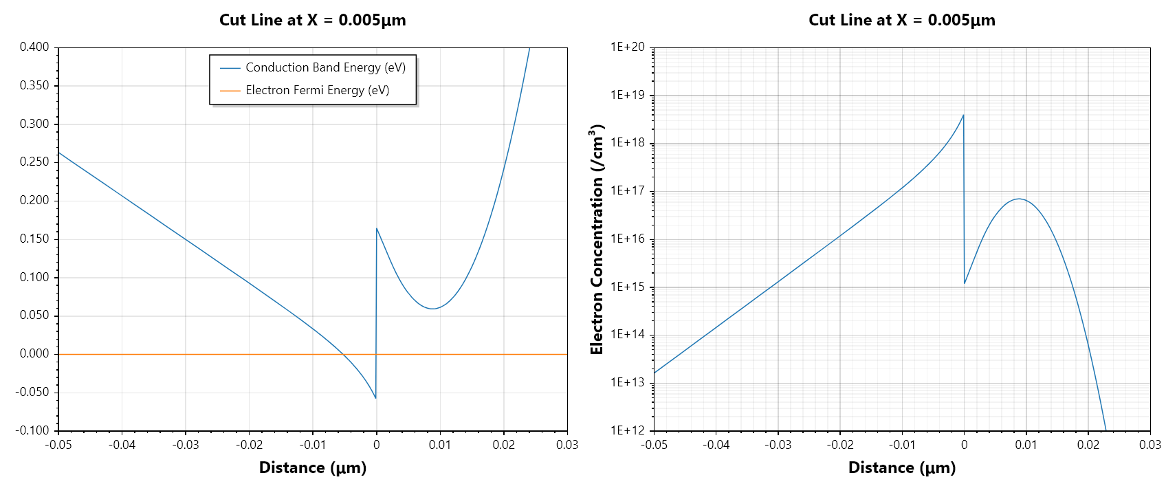
Fig. 7(a). The simulated EC with EF and electron concentration at VG= 0 V.
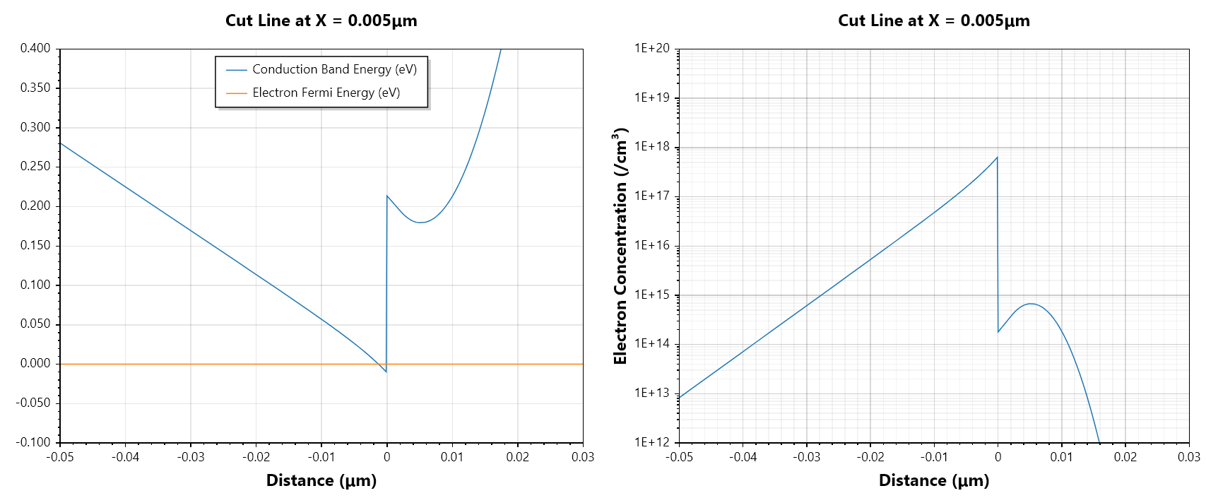
Fig. 7(b). The simulated EC with EF and electron concentration at VG= -0.5 V.
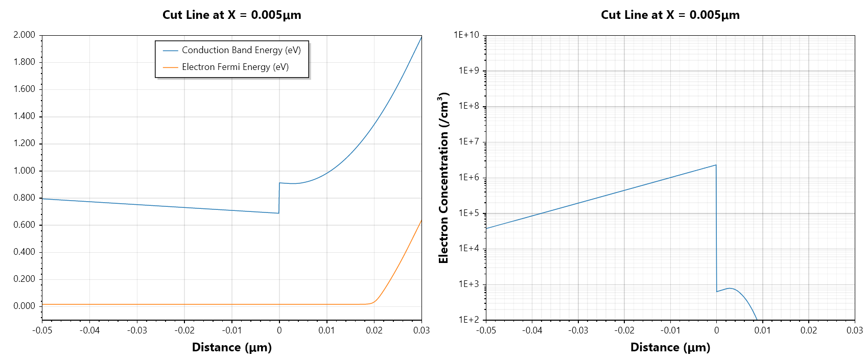
Fig. 7(c). The simulated EC with EF and electron concentration at VG= -1.5 V.
With increasing negative gate bias, as shown in Fig. 7 (b) and (c), the conduction band shifts upward, reducing the electron concentration until the 2DEG channel is fully depleted [3].
For the plots below only the Fermi level for ND = 2E18 cm-3 is shown, since the Fermi-level profiles for the other doping concentrations exhibit negligible variation and are visually indistinguishable on the scale of the plot.
5.2. Varying the Al Mole Fraction
The Aluminium mole fraction in the AlxGa1-xAs directly influences the material bandgap and the conduction band offset at the AlGaAs/GaAs heterostructure. In Aquarius TCAD, the AlGaAs alloy properties are calculated using Vegard's law from the material parameters defined for AlAs and GaAs. As the aluminium mole fraction is varied, parameters such as the bandgap, dielectric constant, electron affinity, and effective mass are adjusted accordingly. As an example, the bandgap relationship used for the AlGaAs is shown below:
The conduction band-edge energy profiles and electron concentration with varied mole fraction (X=0.2, 0.3 and 0.4) are shown in Fig. 8 (a) and (b), when the gate voltage is 0 V.
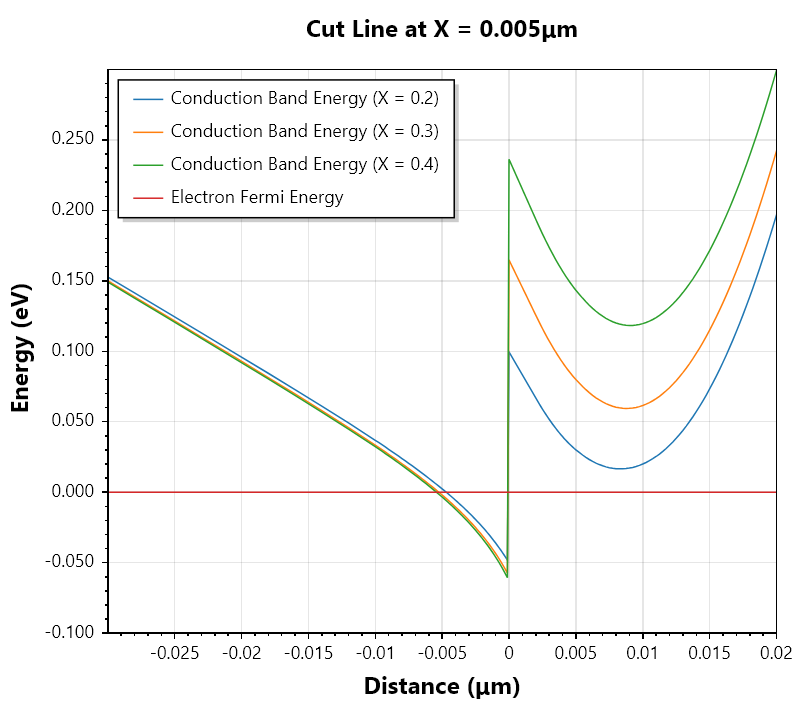
Fig. 8(a). Conduction Band and Fermi Energy at VG= 0 V.
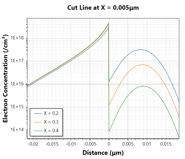
Fig. 8(b). Electron concentration with varied Al mole fraction (X=0.2, 0.3 and 0.4).
As the mole fraction X increases, the AlGaAs bandgap becomes larger, raising the conduction band edge and increasing the conduction band discontinuity at the AlGaAs/GaAs interface (see Fig. 8(a)). This results in a deeper potential well on the GaAs side, where the 2DEG forms, leading to increased electron confinement and a higher electron concentration (see Fig. 8(b)).
While increasing the aluminium mole fraction boosts the conduction band offset and 2DEG concentration, excessively high Al content degrades carrier transport due to heightened DX-centre effects and reduced mobility. Beyond X = 0.45, AlGaAs transitions into an indirect-bandgap material [4-5]. Consequently, practical HEMT devices typically employ an aluminium composition around X = 0.3 to strike an optimal balance between electron confinement and transport properties. Although simulations may show continued performance gains at higher mole fractions, accurately modelling devices beyond this threshold requires additional physical models to capture these bandgap and defect transitions.
5.3. Varying the Doping Concentration
Fig. 9 presents the conduction-band-edge energy profiles and electron concentrations for various doping levels in the Al0.3Ga0.7As layer at a gate voltage of 0 V.
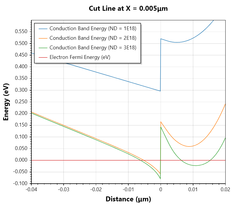
Fig. 9(a). Conduction-band edge and Fermi-level profiles at VG = 0 V for varying donor concentrations.
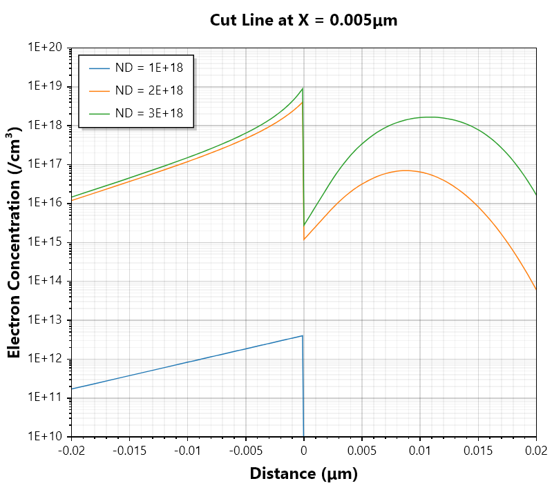
Fig. 9(b). Electron concentration profiles at VG = 0 V or varying donor concentrations.
As shown in Figs. 9(a) and 9(b), increasing the donor concentration in the AlGaAs layer results in stronger band bending at the AlGaAs/GaAs interface, leading to a deeper potential well and a higher electron concentration in the 2DEG. However, the increased density of ionised donors, evident from the enhanced band bending on the AlGaAs side of the heterointerface, also increases Coulomb scattering, which can degrade carrier mobility [2]. Conversely, at lower doping concentrations, the band bending is insufficient to bring the conduction band below the Fermi level, and no 2DEG forms under zero-bias conditions.
5.4. Varying the Schottky Work Function
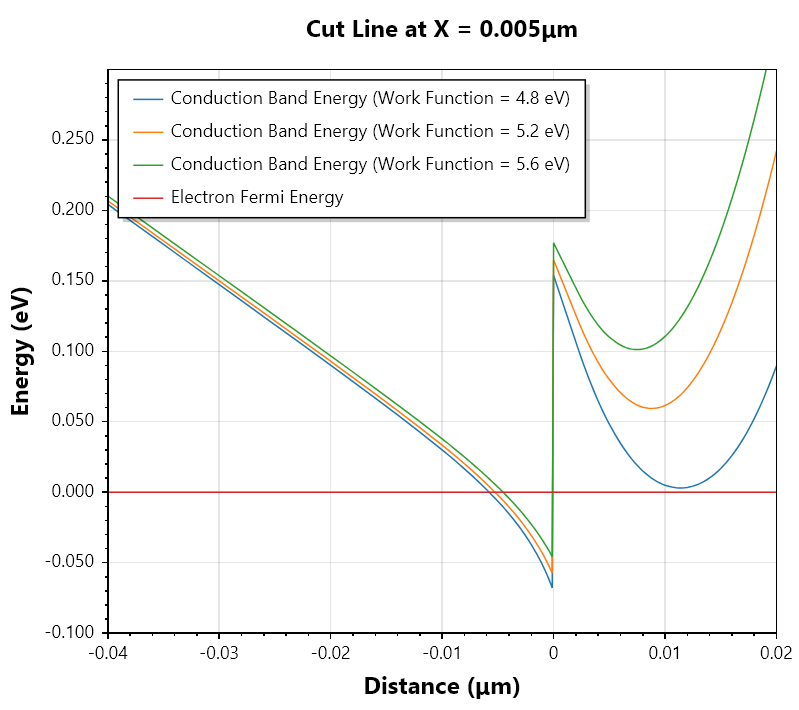
Fig. 10(a). Conduction-band edge and Fermi-level profiles at VG = 0 V for varying Schottky metal work functions.
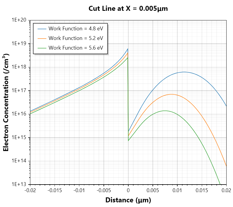
Fig. 1(b). Electron concentration profiles at VG = 0 V for varying Schottky metal work functions.
The Schottky-gate metal work function influences the surface potential and conduction-band bending, as shown in Fig. 10(a). At zero bias, a lower work function enhances band bending and promotes channel formation, whereas a higher work function reduces band bending, making channel formation more difficult. The corresponding electron concentration profiles are shown in Fig. 10(b).
5.5. Incomplete Ionisation
To evaluate the influence of DX centers in the Al0.3Ga0.7As donor layer (ND = 2E+18 cm-3) [3], simulations were performed with and without the incomplete ionisation model. The resulting conduction band edge and electron concentration profiles are shown in Fig. 11 (a) and (b), respectively.
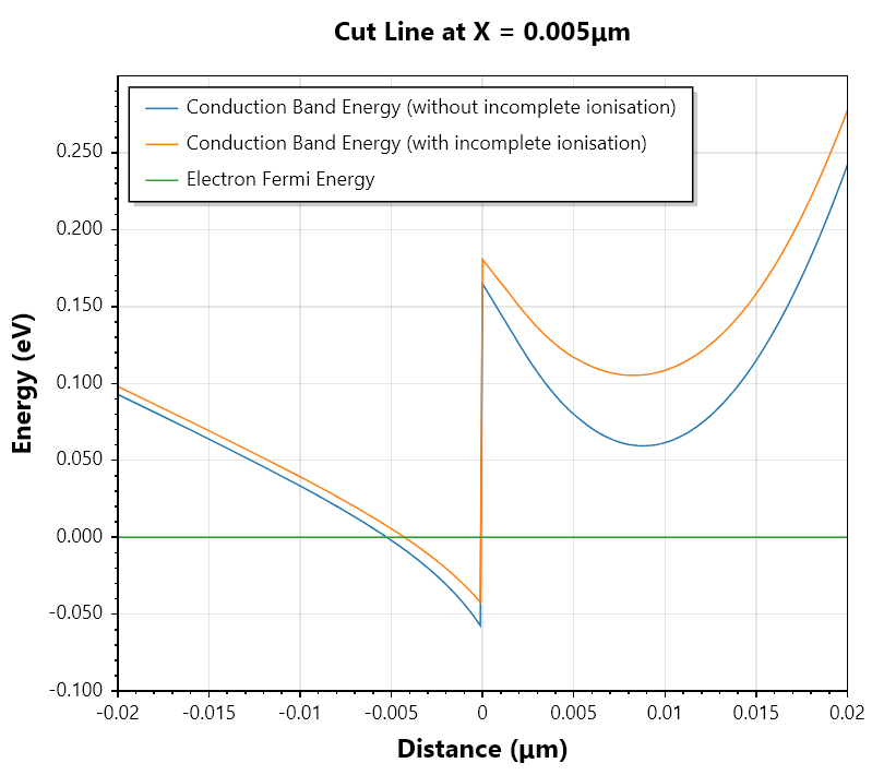
Fig. 11(a). Conduction Band and Fermi Energy at VG = 0 V with incomplete ionisation model and without.
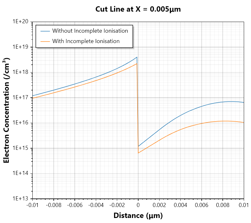
Fig. 11(b). Electron concentration at VG= 0 V with incomplete ionisation model and without.
The inclusion of the incomplete ionisation model reduces the number of ionized donors in the AlGaAs layer. As a result, less positive charge is present in the donor layer, leading to weaker conduction band-edge bending and a shallower potential well at the AlGaAs/GaAs interface (see Fig. 11 (a)). Thus, reducing the electron concentration in the 2DEG channel, as shown in Fig. 11 (b).
6. Conclusion
In this application note, an AlGaAs/GaAs 1D heterostructure was successfully modelled in Aquarius TCAD, capturing the formation and control of the 2DEG channel. The influence of Al mole fraction, donor concentration, Schottky gate work function and incomplete ionisation on the conduction band-edge profile and electron concentration was investigated. The results demonstrate the key physical mechanisms governing 2DEG formation in AlGaAs/GaAs heterostructures.
7. References
[1] J.P. Colinge and C. A. Colinge, Physics of Semiconductor Devices. New York, NY, USA: Springer, 2002, pp. 315–330.
[2] P. Paramasivam, N. Gowthaman, and V. M. Srivastava, “Self-consistent Analysis for Optimization of AlGaAs/GaAs Based Heterostructure,” Journal of Electrical Engineering & Technology, vol. 19, pp. 4469–4483, 2024, doi: 10.1007/s42835-023-01721-7.
[3] H. Mizuta, K. Yamaguchi, M. Yamane, T. Tanoue and S. Takahashi, "Two-dimensional numerical simulation of Fermi-level pinning phenomena due to DX centers in AlGaAs/GaAs HEMTs," in IEEE Transactions on Electron Devices, vol. 36, no. 10, pp. 2307-2314, Oct. 1989, doi: 10.1109/16.40915
[4] L. Aucoin, “HEMTs and PHEMTs,” in GaAs MMIC Reliability Assurance Guideline for Space Applications, Jet Propulsion Laboratory (JPL), Pasadena, CA, USA, 1996, ch. IV, pp. 39–43. Available: https://parts.jpl.nasa.gov/mmic/3-IV.PDF
[5] K. Maezawa, “Barrier Height in Indirect Bandgap AlGaAs/GaAs Hetero-Junction Determined with n-Semiconductor/Insulator/Semiconductor Diodes,” Jpn. J. Appl. Phys., vol. 25, p. L557, 1986.20461