Bipolar Junction Transistor (BJT)
1. Abstract
This application note describes the simulation of the Silicon bipolar junction transistor (BJT) device, which includes the output characteristics and gain, extracted from the gummel plot, as well as the blocking characteristics.
2. Introduction
The invention of the bipolar junction transistor (BJT) in 1947 marked the beginning of modern solid-state electronics. Since then, BJTs have been widely used in a variety of applications, including analogue circuits, high-speed circuits (RF), and power electronics [1-2]. There are two main types of BJTs: NPN (with a p-type base) and PNP (with an n-type base). In this application note, the focus is on the NPN transistor. As described in [1], the BJT operates by using a small base current to control a much larger current flowing between the emitter and the collector. This behaviour, known as transistor action, occurs when the base–emitter junction is forward biased and the base–collector junction is reverse biased.
For integrated circuit applications, the lateral NPN BJT, in which all three terminals are located at the surface, as illustrated in Fig. 1(a). The device is fabricated on a p-type substrate, with dielectric-filled trenches (SiO₂) used to isolate neighbouring devices. The buried collector–substrate junction is typically reverse biased to ensure proper device isolation. The transistor itself is formed within a lightly doped n-type epitaxial layer. The transistor action takes place between the highly doped N⁺ emitter, the p-type base (which is contacted through a heavily doped P⁺ region to ensure a good ohmic contact), and the collector region, which consists of a lightly doped collector and a highly doped N⁺ contact region to reduce contact resistance.
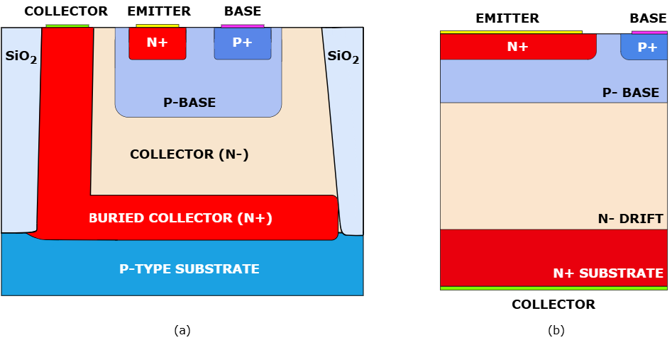
Fig. 1. BJT devices: (a) device for integrated circuits; (b) device for power or small-signal applications.
In contrast, a vertical NPN BJT, used in small-signal and power applications [2], is shown in Fig. 1 (b). Unlike the lateral device, the substrate is highly doped N⁺, and the active device is formed on a thick, lightly doped epitaxial layer that acts as a drift region. This region enables the device to support low-to-medium breakdown voltages (typically in the range of 50–1000 V).
In this application note, the structure shown in Fig. 1 (a) is simplified, based on the example in [1], in order to evaluate its static performance.
3. Device Structure
3.1. Geometry
The schematic of the simulated BJT device is shown in Fig. 2 (a) with its key structural parameters (also summarised in Table 1) and the simulated meshed device is shown in Fig. 2 (b). Note, for better simulation accuracy the additional mesh box was included in the active region of the BJT (around the emitter-base and base-collector junctions), where steep carrier and electric field gradients occur and strongly influence current transport and junction behaviour. Additionally, the mesh refinement options for the grid mesh type are shown in Table 2.
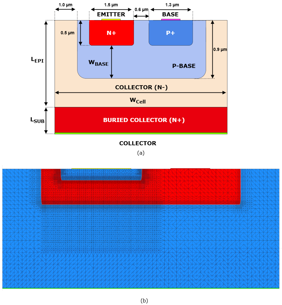
Fig. 2. BJT representations: (a) schematic; (b) meshed device generated in the device model (.sdm) file.
Table 1: BJT parameters
| Parameter | Symbol | Value | Unit |
|---|---|---|---|
| ½ Cell width | WCELL | 7 | µm |
| Epitaxial layer thickness | LEPI | 2 | µm |
| Substrate thickness | LSUB | 1 | µm |
| Base width | WBASE | 0.4 | µm |
| Collector doping concentration | N- | 2.0E+15 | cm-3 |
| Buried collector doping concentration | N+ | 7.0E+17 | cm-3 |
Table 2: Mesh Refinement Options
| Setting | Value |
|---|---|
| Number of Iterations | 2 |
| Refinement Variable | Distance from Junction |
| Distance (Microns) | 0.2 |
| Reduction Factor | 0.5 |
3.2. Doping Profiles
The N⁺ emitter (0.5 µm deep) with P⁺ (0.5 µm deep) and P-base (0.9 µm deep) were modelled as the gaussian distribution with the peak doping concentration of 1E+19 cm-3 and 1.2E+18 cm-3, respectively.
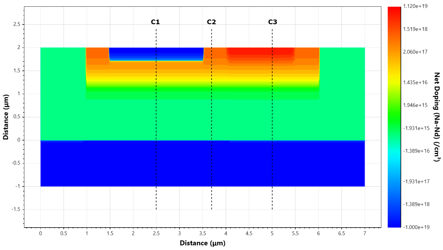
Fig. 3(a). Absolute net doping distribution.
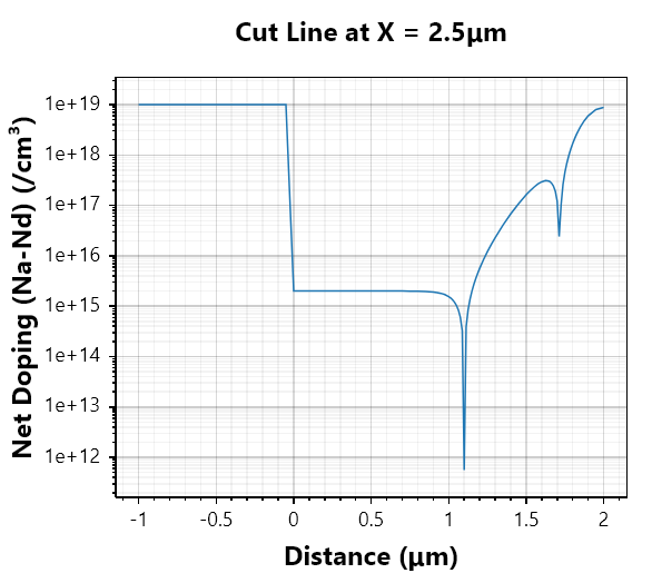
Fig. 3(b). Doping profile along cutline C1.

Fig. 3(c). Doping profile along cutline C2.
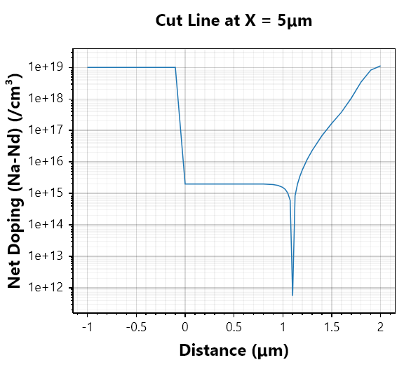
Fig. 3(d). Doping profile along cutline C3.
Using the Results Visualizer tool, the doping concentration profiles (Net doping) through N⁺ emitter (vertical cutline C1 @ 2.5 µm), P⁺ base (C2 @ 3.7 µm) and the P-base (C3 @ 5µm) are shown in Fig. 3.
4. Simulation results
In this section the Aquarius TCAD circuit and device simulator is used to evaluate the device gain through plotting the base and collector currents, as a function of the emitter-base voltage (Gummel plot). As well as the output characteristics as a function of the base current.
For the simulations performed, the parameters of the Shockley–Read–Hall (SRH) lifetime model are listed in Table 3. The corresponding electron and hole lifetimes as a function of the doping concentration are shown in Fig. 4.
For more detailed information on SRH, click here.
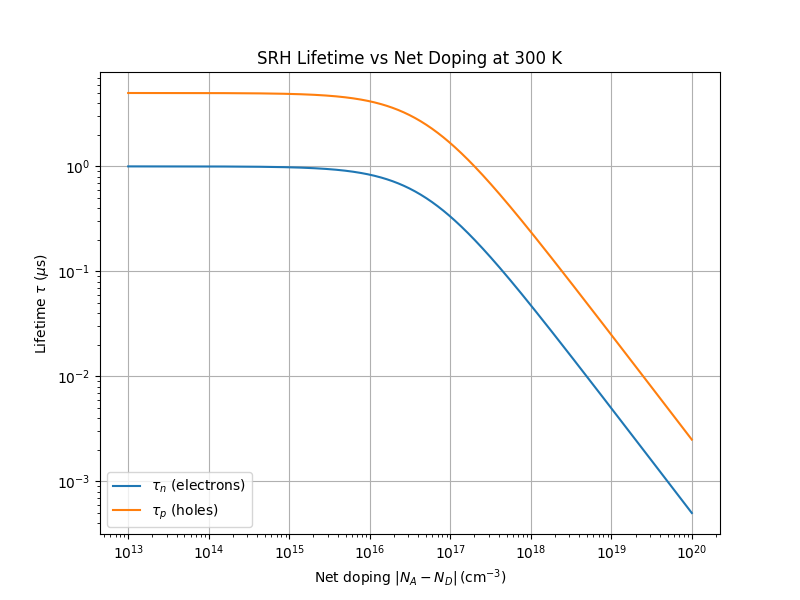
Fig. 4. SRH electron and hole lifetimes as a function of doping concentration.
Table 3: SRH lifetime parameters
| Parameter | Value | Units |
|---|---|---|
E_TRAP | 0 | eV |
SRH_TAU_P | 5E-06 | s |
SRH_AP | 1 | - |
SRH_BP | 1 | - |
SRH_CP | 0 | - |
SRH_DP | 0.5 | - |
SRH_NREFP | 5E16 | cm-3 |
SRH_TAU_N | 1E-06 | s |
SRH_AN | 1 | - |
SRH_BN | 1 | - |
SRH_CN | 0 | - |
SRH_DN | 0.5 | - |
SRH_NREFN | 5E16 | cm-3 |
For the off-state and breakdown voltage simulations, the impact ionisation model (Chynoweth, Element) using the default Si parameters was included.
4.1. Gummel Plot
To obtain the Gummel plot through simulations, the circuit in Fig. 5 (a) was built in the Circuit Editor and simulation results are shown in Fig. 5 (b). Note, that the simulated area of the device is 0.1 mm².
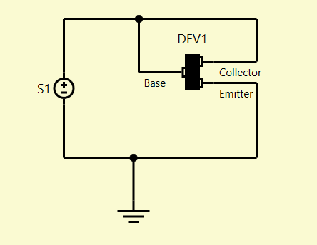
Fig. 5(a). Simulation circuit used to obtain the Gummel plot.
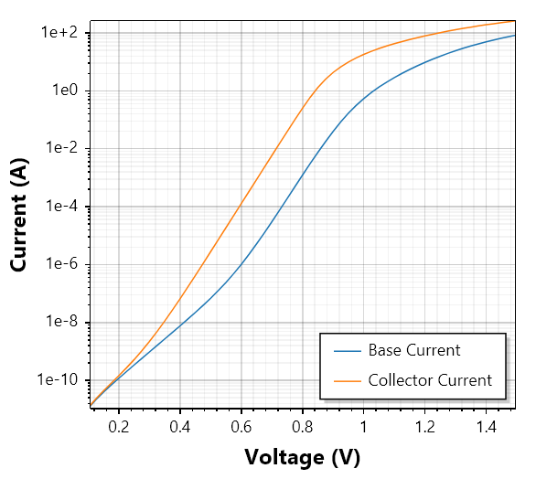
Fig. 5(b). Simulated Gummel plot.
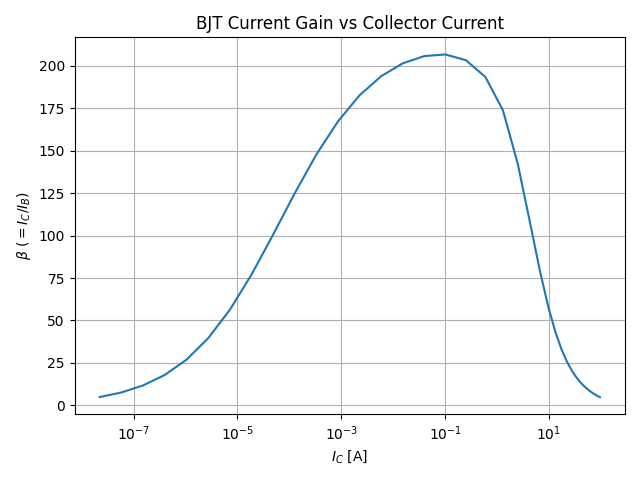
Fig. 6. BJT current gain as a function of collector current.
The calculated gain as a function of the collector current is shown in Fig. 6, with the maximum β of 207 at ICollector= 0.1A.
Additionally, the electron and hole concentrations were recorded along cut line C1 at base–collector voltages of 0.6 V, 0.8 V, and 1 V (see Fig. 3 for reference) and are shown in Fig. 7. As the base–emitter voltage increases, the injected carrier concentration in the collector drift region rises significantly. When the injected electron concentration becomes comparable to or exceeds the background doping of the drift region, conductivity modulation occurs. At such high current densities, the associated stored charge contributes to gain degradation (see Fig. 6, reduction in β for IC ≳ 1" A" ), which is consistent with the onset of the Kirk effect (base push-out) [1].
As a result, a trade-off exists between improved carrier transport through the collector region and increased stored charge. In power devices, conductivity modulation is often desirable because it reduces conduction losses. However, in small-signal or RF transistors, excessive carrier storage degrades high-frequency performance and switching speed.
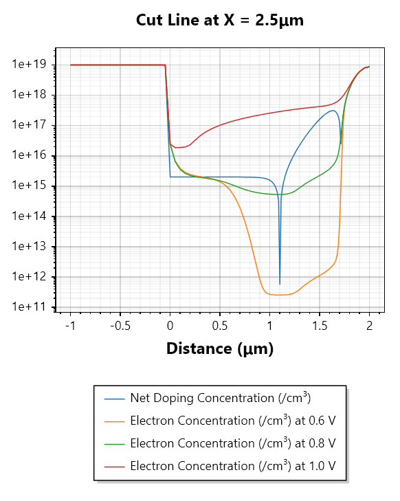
Fig. 7(a). Electron concentration at different base–collector voltages.
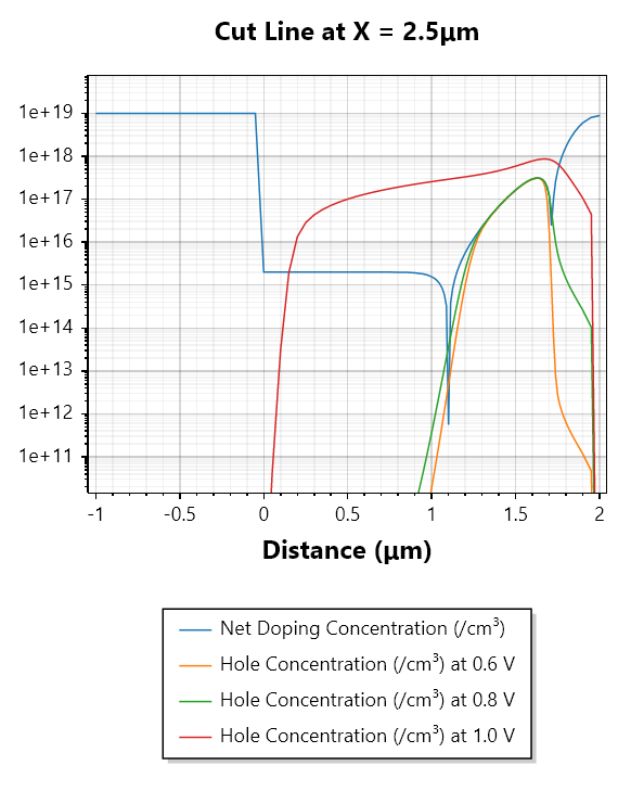
Fig. 7(b). Hole concentration at different base–collector voltages.
4.2. Output characteristics
To simulate the output characteristics, the circuit shown in Fig. 8 (a) was constructed. First, the desired base voltage was applied, which passes through a 10 kΩ resistor (acting as an equivalent current source to obtain the required base current. Using the simulation results from this first step as the initial conditions, the collector voltage was then swept in the second step between 0 V and 5 V.
For more detailed information on loading initial conditions, click here.
Base voltages of 5 V, 10 V, and 15 V were applied, resulting in base currents of 0.42 mA, 0.9 mA, and 1.42 mA, respectively. The simulation results corresponding to these base currents are shown in Fig. 8 (b).
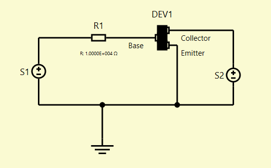
Fig. 8(a). Simulation circuit used to obtain output characteristics.
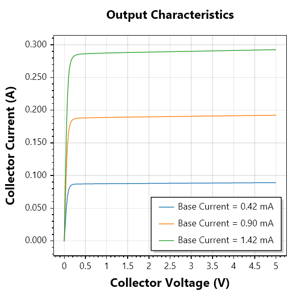
Fig. 8(b). Simulated BJT output characteristics.
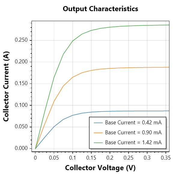
Fig. 8(c). Zoomed-in view of the saturation region.
4.3. Blocking Voltage characteristics
Although the device structure used in this work is based on the simplified example presented in [1], it resembles a vertical BJT with a lightly doped collector drift region. Therefore, in addition to the on-state characteristics, the off-state behaviour of the device is also investigated.
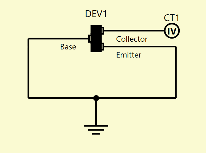
Fig. 8(a). Simulation circuit used to obtain off-state characteristics.
Table 4: Curve Tracer parameters
| Parameter | Value |
|---|---|
| Start Voltage (V) | 0 |
| Initial Step (V) | 0.1 |
| Minimum Voltage (V) | 0.001 |
| Maximum Voltage (V) | 200 |
| Minimum Current (A) | 1E-06 |
| Maximum Current (A) | 0.01 |
| Minimum Newton | 6 |
| Maximum Newton | 8 |
| Current Increment Factor | 2 |
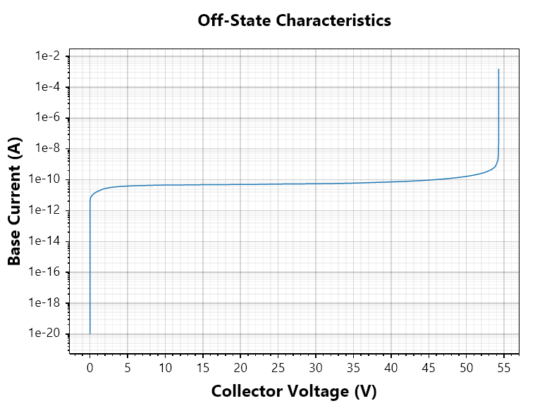
Fig. 10. Simulated reverse current characteristics.
To simulate the off-state characteristics, the circuit configuration using the curve tracer setup with curve tracer parameters are shown in Fig. 9 and Table 4. The simulated reverse current is shown in Fig. 10. In this configuration both Emitter and Base are shorted ( BVCES ) [2].
For more information see IV Curve Tracer.
The simulated BVCES is approximately 54 V. The electric field distribution at 40 V and the vertical cutline located at 1.1 µm (Fig. 11 (a) and (b)) shows that the depletion region remains confined within the collector–base junction, indicating that the base doping and width are sufficient to prevent punch-through.
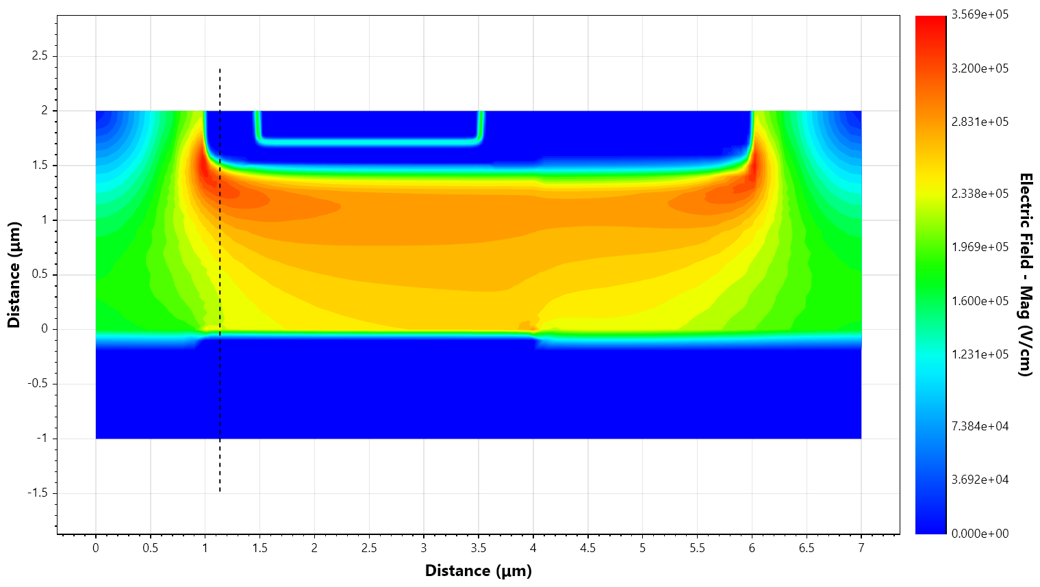
Fig. 11(a). Electric field distribution recorded at VC = 40 V.
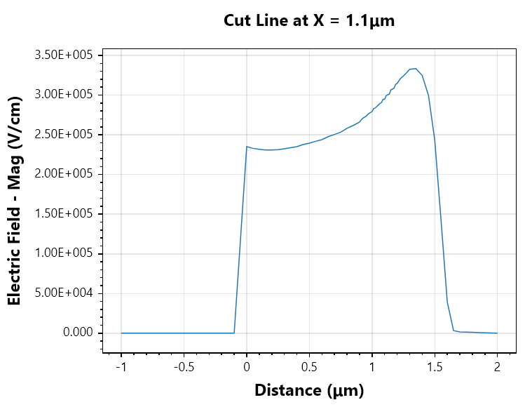
Fig. 11(b). Electric field cutline through X = 1.1 µm at VC = 40 V.
5. Conclusion
In this application note, the static behaviour of a silicon NPN BJT was analysed using the Aquarius TCAD tool. The device structure and doping profiles were built using the Device Editor, and the transistor performance was evaluated through Gummel, output, and off-state characteristic simulations. The results demonstrate the expected transistor behaviour.
6. References
[1] J. P. Colinge and C. A. Colinge, Physics of Semiconductor Devices. New York, NY, USA: Springer, 2002.
[2] B. J. Baliga, Fundamentals of Power Semiconductor Devices. New York, NY, USA: Springer, 2008.