Insulated Gate Bipolar Transistor (IGBT)
1. Abstract
This application note describes the simulation setup for evaluating the transfer characteristics, output, and off-state behaviour of a silicon insulated gate bipolar transistor (IGBT) designed for 1200 V rated voltage operation.
2. Introduction
Insulated gate bipolar transistors (IGBTs) have been widely used since their introduction in the 1980s, largely replacing bipolar power transistors, which are complex to design for high-voltage operation. Today, IGBTs serve as the workhorse of many power electronic applications in both DC and AC systems. Commercially available devices typically cover a voltage range from approximately 750 V to 6.5 kV and are widely used in automotive, traction, and energy applications [1].
An IGBT is a three-terminal device consisting of a gate, emitter, and collector. As described in [1], it can be conceptually represented by an equivalent circuit comprising a PNP bipolar transistor driven by a MOSFET. Based on their gate structure, vertical IGBTs are generally classified into planar-gate and trench-gate types.
They can also be categorised as punch-through (PT) and non-punch-through (NPT) devices [1-2]. Planar-gate IGBTs are simpler to fabricate but exhibit higher on-state resistance due to the presence of an additional JFET region and a larger cell pitch compared to trench-gate designs. The distinction between punch-through (PT) (see Fig. 1(a)) and non-punch-through (NPT) (see Fig. 1(b)) structures lies primarily in the collector-side design, specifically in whether an n-type buffer layer is included.
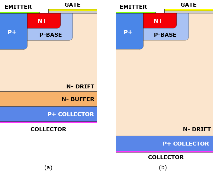
Fig. 1. IGBT half-cell schematics: (a) PT design; (b) NPT design.
PT-IGBTs incorporate the n-buffer layer, enabling a thinner drift region, whereas NPT devices require a thicker drift region to avoid punch-through.
Additionally, the PT-IGBT design can employ a thinned P+ collector to further reduce the forward voltage drop. This structure is adapted from [3-4] and used in the simulations presented in this application note.
3. Device Structure
3.1. Geometry
The schematic of the simulated IGBT device is shown in Fig. 2, with its key structural parameters (also summarised in Table 1) and the simulated meshed device is shown in Fig. 2 (b). Additionally, the mesh refinement options for the grid mesh type are shown in Table 2. Note, that the N-drift and P-collector were modelled as constant doping concentration regions.
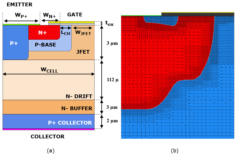
Fig. 2. (a) IGBT half-cell schematic; (b) zoomed-in view of the active area showing the device mesh from the .sdm file.
Table 1: IGBT model parameters
| Parameter | Symbol | Planar | Unit |
|---|---|---|---|
| ½ Cell width | WCELL | 3.5 | µm |
| P+ width | WP+ | 0.8 | µm |
| N+ width | WN+ | 0.8 | µm |
| JFET width | WJFET | 1.3 | µm |
| Channel length | LCH | 0.6 | µm |
| Gate oxide thickness | tox | 100 | nm |
| N-drift doping concentration | — | 5E+13 | cm-3 |
| P+ collector doping | — | 7E+17 | cm-3 |
Table 2: Mesh Refinement Options
| Setting | Value |
|---|---|
| Number of Iterations | 2 |
| Refinement Variable | Distance from Junction |
| Distance (Microns) | 0.4 |
| Reduction Factor | 0.5 |
3.2. Doping Profiles
The JFET, P-base, P⁺, N⁺ and N-buffer regions were modelled using Gaussian doping profiles, with the openings listed in Table 1 representing the mask windows through which implantation is performed.
To approximate lateral diffusion effects, a reduction factor of 0.5 was applied to the lateral profile. The summary of the peak doping concentration and depth of modelled Gaussian profiles is displayed in Table 3.
Table 3: IGBT Gaussian profiles parameters
| Profile | Peak Doping Concentration (cm-3) | Profile Depth (µm) |
|---|---|---|
| N-JFET | 2.0E+16 (@ 115 µm) | 3.0 |
| P-base (channel) | 2.7E+17 (@ 115 µm – channel) | 2.5 |
| P-base | 2.7E+17 (@ 113.8 µm) | 2.5 |
| P+ emitter | 1.0E+19 (@ 115 µm) | 3.0 |
| N+ emitter | 1.0E+20 (@ 115 µm) | 0.5 |
| N-buffer | 2.0E+16 (@ -3 µm) | 6.0 |
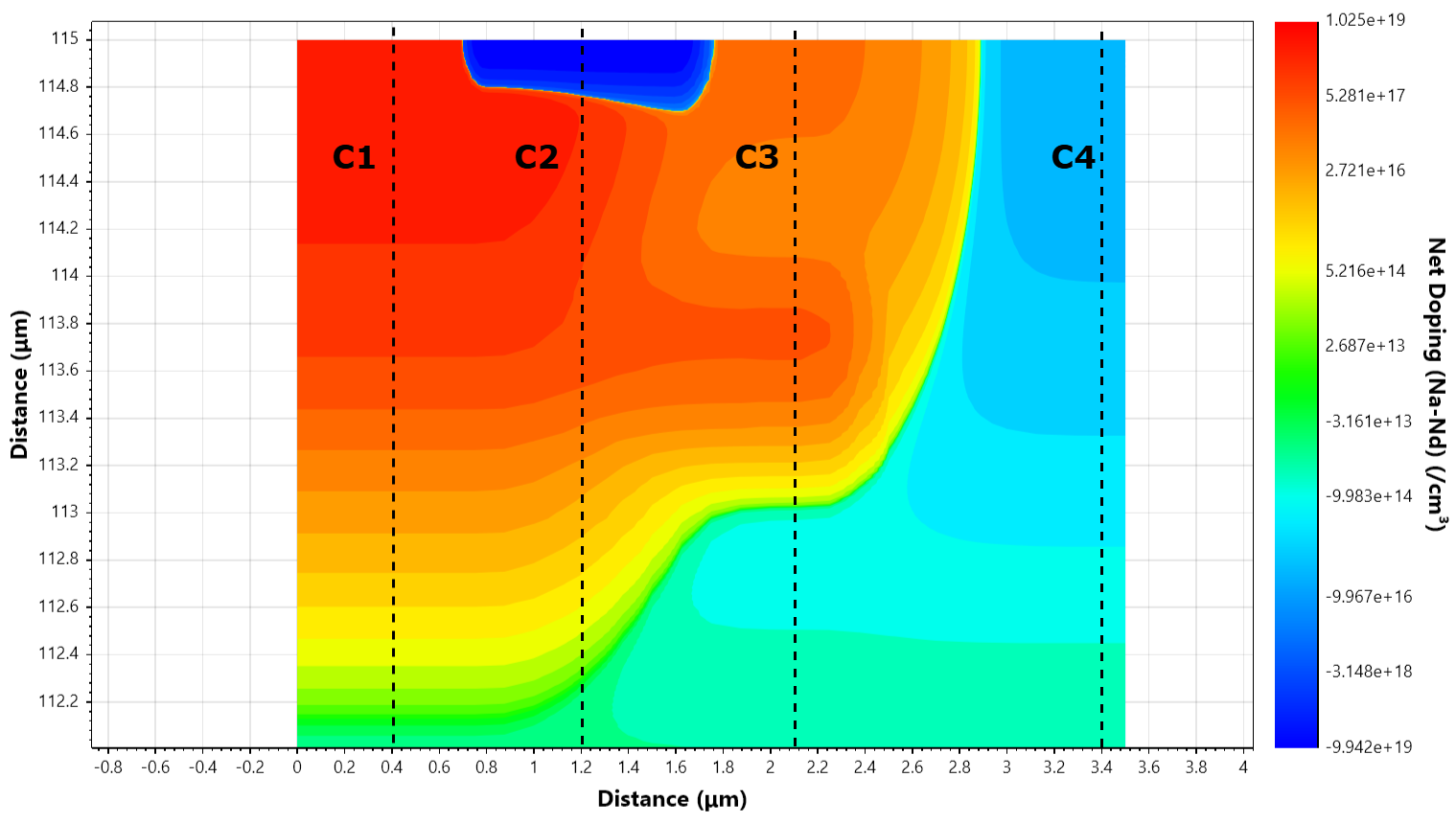
Fig. 3. (a) Contour plot of the net doping concentration in the active region of the device (zoomed view).
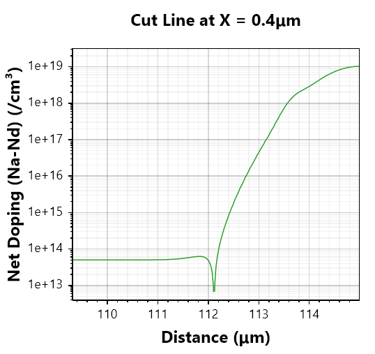
Fig. 3. (b) Absolute Net Doping profile along cutline C1.
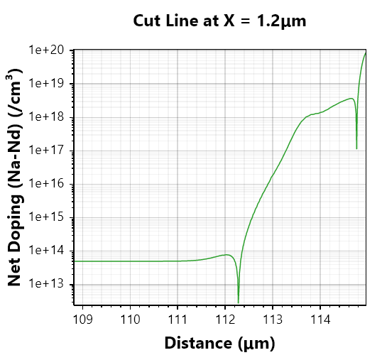
Fig. 3. (c) Absolute Net Doping profile along cutline C2.
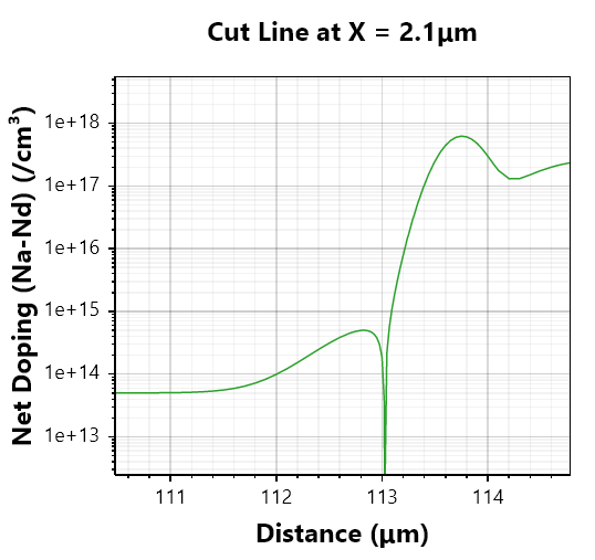
Fig. 3. (d) Absolute Net Doping profile along cutline C3.
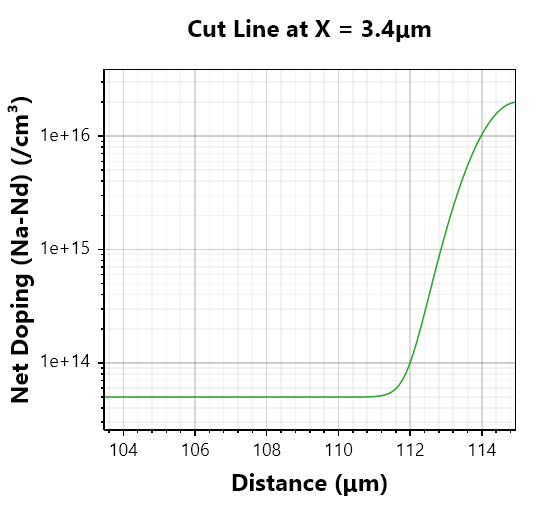
Fig. 3. (e) Absolute Net Doping profile along cutline C4.
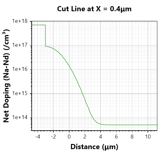
Fig. 3. (f) Doping concentration distribution of the P-collector and N-buffer regions along C1.
4. Simulation results
In this section, the Aquarius TCAD circuit and device simulator is used to evaluate the transfer, output, and off-state characteristics. Similar to the Silicon BJT report, the parameters of the Shockley–Read–Hall (SRH) lifetime model were modified and are listed in Table 4. The corresponding electron and hole lifetimes as a function of the doping concentration are shown in Fig. 4.
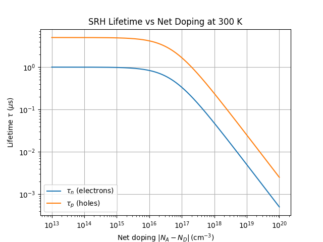
Fig. 4. SRH electron and hole lifetime as a function of the doping concentration.
Table 4: SRH lifetime parameters
| Parameter | Value | Unit |
|---|---|---|
E_TRAP | 0 eV | eV |
SRH_TAU_P | 5E-06 | s |
SRH_AP | 1 | - |
SRH_BP | 1 | - |
SRH_CP | 0 | - |
SRH_DP | 0.5 | - |
SRH_NREFP | 5E+16 | cm-3 |
SRH_TAU_N | 1E-06 | s |
SRH_AN | 1 | - |
SRH_BN | 1 | - |
SRH_CN | 0 | - |
SRH_DN | 0.5 | - |
SRH_NREFN | 5E+16 | cm-3 |
The off-state and breakdown voltage simulations the Chynoweth model (Element) with default Si parameters was used.
4.1. Transfer Characteristics
To simulate the transfer characteristics, the circuit shown in Fig. 5 (a) was constructed. The collector voltage (VCE) was first swept from 0 to 2 V. The solution from the first step was then used as the initial condition for the gate voltage (VGE) sweep from 0 to 20 V.
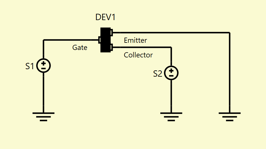
Fig. 5. (a) Simulation circuit for transfer characteristics.
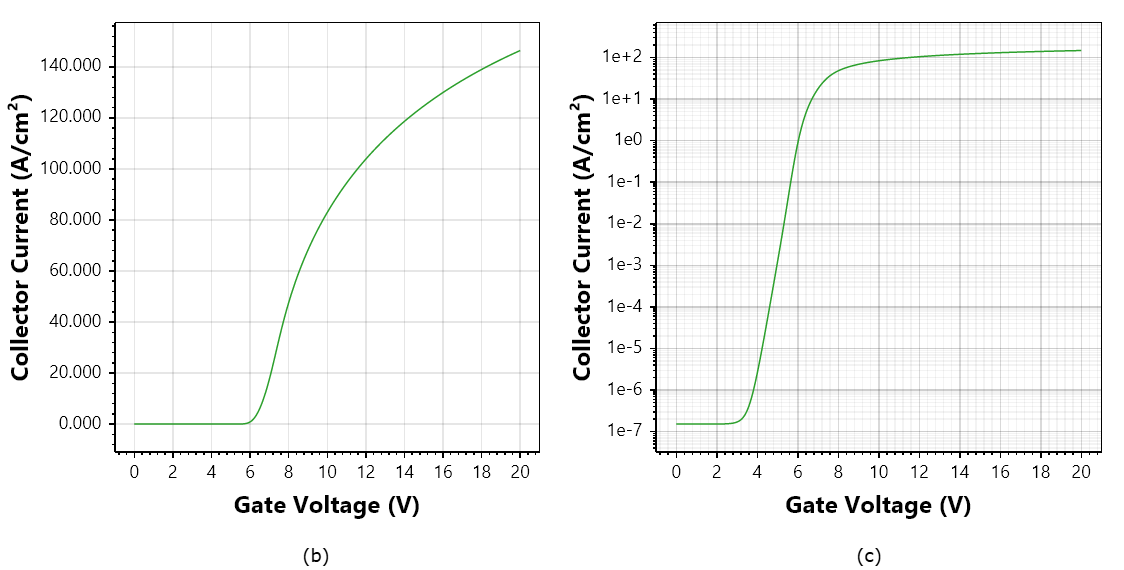
Fig. 5. (b) Simulated transfer characteristics (linear scale); (c) simulated transfer characteristics (logarithmic scale).
For more detailed information on loading initial conditions, click here.
4.2. Output Characteristics
To simulate the output characteristics, the circuit shown in Fig. 6 (a) was constructed. The gate voltage (VGE) was first swept from 0 V to the target voltage. The solution from the first step was then used as the initial condition for the collector voltage (VCE) sweep from 0 to 4 V.
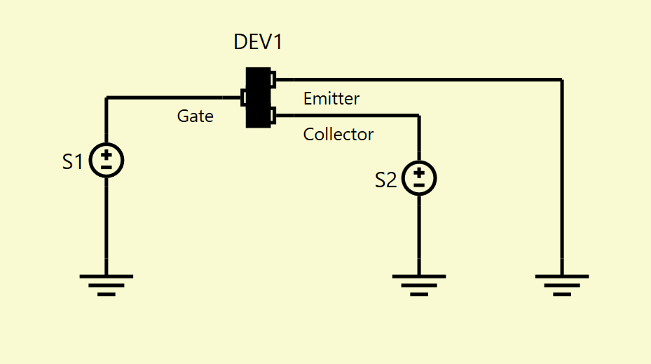
Fig. 6(a). Simulation circuit for output characteristics.
The simulated output characteristics for varying VGE (12–18 V in increments of 3 V) are shown in Fig. 6 (b). The on-state voltage VCE , sat is defined as the collector–emitter voltage at a current density of 100 A/cm² and VGE = 15V, is 1.75 V.
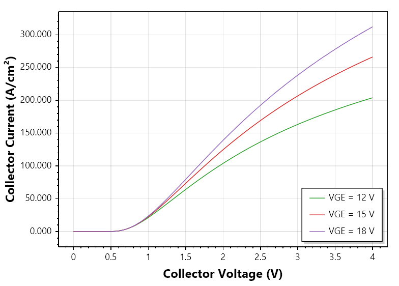
Fig. 6. (b) Simulated output characteristics for VGE = 12 V, 15 V, and 18 V.
Additionally, the current distribution at JC=100 A/cm2 is shown in Fig. 6 (c), illustrating current flow bending in the JFET region and the resulting current constriction [1].
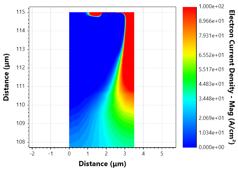
Fig. 6. (c) Current density distribution at VCE=1.75V (JC=100 A/cm2) and V
A vertical cutline at 2.2 µm was taken, and the electron and hole concentrations are shown in Fig. 7. Both carrier concentrations significantly exceed the background drift doping of 5E+13 cm-3, indicating a strong conductivity modulation.
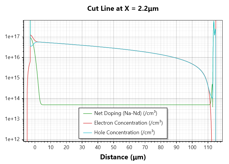
Fig. 7. Electron and hole concentration at VCE=1.75V (JC=100 A/cm2) and VGE=15V.
4.3. Blocking Characteristics
To simulate the off-state characteristics, the circuit configuration using the curve tracer setup. The curve tracer parameters are shown in Fig. 8 and Table 5.
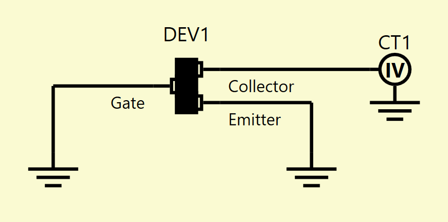
Fig. 8. Circuit for the off-state simulations.
Table 5: Curve Tracer parameters
| Parameter | Value |
|---|---|
| Start Voltage (V) | 0 |
| Initial Step (V) | 0.1 |
| Minimum Voltage (V) | 0.001 |
| Maximum Voltage (V) | 2500 |
| Minimum Current (A) | 1E-06 |
| Maximum Current (A) | 0.01 |
| Minimum Newton | 6 |
| Maximum Newton | 8 |
| Current Increment Factor | 2 |
For more information see IV Curve Tracer.
The simulated reverse leakage current is shown in Fig. 9 (a), indicating a maximum blocking voltage of 1710 V. The electric field (EF) distribution at 1200 V is shown in Fig. 9(b), demonstrating a well-protected top-emitter region, with the gate oxide electric field remaining well below 0.5 MV/cm.
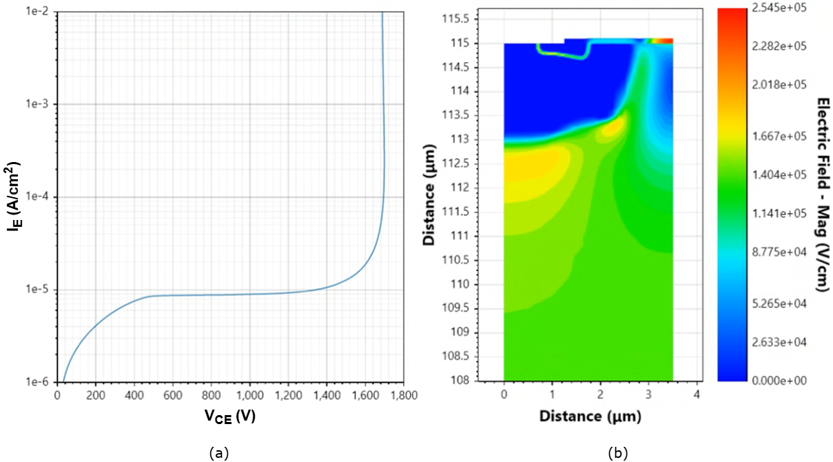
Fig. 9. (a) Simulated reverse leakage current; (b) contour plot of the electric field distribution at 1.2 kV.
Additionally, the electric field profile along a vertical cutline at 0 μm, recorded at 1200 V, is shown in Fig. 10. The profile exhibits the characteristic trapezoidal shape of a PT-IGBT design. A small electric field peak is observed at the N-buffer/P-collector junction, attributed to the depletion region formed at the forward-biased p–n junction.
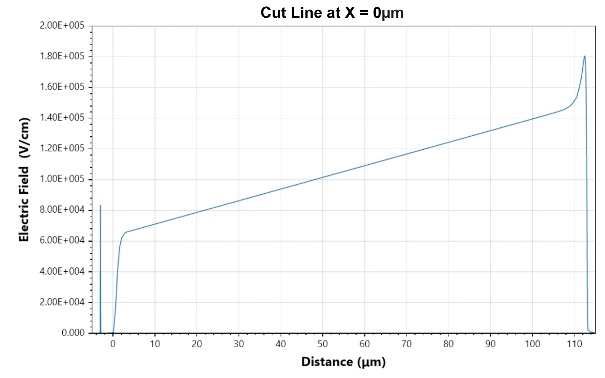
Fig. 10. Electric Field profile recorded at 1200 V.
5. Conclusion
In this application note, the static behaviour of a silicon punch-through (PT) IGBT was analysed using the Aquarius TCAD tool. The device structure and doping profiles were constructed using the Device Editor, and the device performance was evaluated through transfer, output, and off-state characteristic simulations. The results demonstrate the expected IGBT behaviour, including strong conductivity modulation and high-voltage blocking capability.
6. References
[1] B. J. Baliga, Fundamentals of Power Semiconductor Devices. New York, NY, USA: Springer, 2008.
[2] Toshiba Electronic Devices & Storage Corporation, IGBTs (Insulated Gate Bipolar Transistor) Application Note, Jul. 4, 2022.
[3] M. Antoniou, F. Udrea and F. Bauer, "The Superjunction Insulated Gate Bipolar Transistor Optimization and Modeling," in IEEE Transactions on Electron Devices, vol. 57, no. 3, pp. 594-600, March 2010, doi: 10.1109/TED.2009.2039260.
[4] M. Tanaka and I. Omura, “IGBT scaling principle toward CMOS compatible wafer processes,” Solid-State Electronics, vol. 80, pp. 118–123, 2013, doi: 10.1016/j.sse.2012.10.020.